
Hook
What is a SoC?
A System‑on‑Chip integrates multiple hardware IP blocks:
- CPU (general purpose): Arm, x86 or RISC‑V cores run the OS and control logic.
- GPU: massively parallel compute (graphics, GPGPU, AI kernels).
- NPU/VPU/DSP: dedicated accelerators (neural networks, vision, audio/video, signal processing).
- Memory subsystem: DDR/LPDDR controllers, cache hierarchy, coherency fabrics.
- Interconnect: AMBA/AXI networks or a NoC (network‑on‑chip).
- Peripherals: GPIO, I²C, SPI, UART, PWM, USB, Ethernet, PCIe, MIPI CSI/DSI, CAN.
- Security: secure boot, TEEs, crypto engines.
- Power & clocks: DVFS domains, PLLs, low‑power states.
Why it matters
- Energy efficiency: short data paths → lower dynamic power.
- Low latency: on‑chip hops beat board‑level detours.
- BOM/footprint: fewer chips, smaller boards, lower cost.
- Performance‑per‑watt: the key metric for edge and embedded.
The big families of SoCs (with examples)
- Application Processors (AP): multi‑core CPU + GPU + ISPs + accelerators. Examples: Raspberry Pi 5 (BCM2712), Qualcomm Snapdragon, NXP i.MX 8, Apple M‑series.
- MCU‑class SoCs: lightweight CPUs with on‑chip SRAM/Flash and tight real‑time I/O. Examples: STM32, ESP32.
- AI/Vision SoCs: purpose‑built NPUs/VPUs. Examples: NVIDIA Jetson (Orin/Xavier), Intel Movidius, Google Coral (Edge TPU), ARM NPUs.
- SoC‑FPGAs: CPU + FPGA on one die for cycle‑accurate logic. Examples: Xilinx Zynq/Versal, Intel Agilex SoC.
- Industrial/real‑time SoCs: determinism, functional safety, field buses (CAN, TSN). Examples: TI Sitara AM62/AM64, Renesas families.
Metaphor: think airports. APs are global hubs; MCUs are agile airfields; Jetson/Coral are cargo terminals for AI; SoC‑FPGAs are modular airports where you can draw your own runways.
How software actually runs on a SoC
- Boot stack: Boot ROM → bootloader → kernel (Linux/RTOS) → drivers/services → app.
- Acceleration: schedulers and drivers dispatch work across CPU/GPU/NPU/DSP.
- Physical I/O: drivers expose GPIO/buses/timers; DMA moves buffers off‑CPU.
- Energy control: DVFS and power‑gating scale voltage/frequency per domain.
The plumbing: GPIO, buses, DMA, and clocks
- GPIO: software‑controlled pins; can be debounced, edge‑triggered, or pulled up/down.
- Buses: I²C, SPI, UART, CAN, MIPI, PCIe, Ethernet/TSN.
- DMA: the conveyor belt that moves data with minimal CPU involvement; supports scatter‑gather.
- Clocks & PLLs: the conductor that sets the tempo; DVFS turns it up during crescendos and down between songs to save energy.
A short history: CPU → GPU → NPU → FPGA
- CPU: from early microprocessors to today’s multi‑core designs, CPUs remain the general‑purpose workhorses.
- GPU: born for 3D, generalized with GPGPU; later, Tensor Cores mainstreamed AI math.
- NPU/TPU/VPU: specialized engines for NN ops (conv, matmul, attention) that maximize perf/W on mobile/edge.
- FPGA & SoC‑FPGA: reconfigurable logic with cycle‑level control; ideal for deterministic pipelines and custom interfaces.
Vendors, SoC families — and how they map to ONNX Runtime EPs
Availability varies by OS/toolchain. Here’s a compact map from SoC vendors/families to ONNX Runtime Execution Providers (EPs) you’d typically use:

Key idea: a single ONNX graph can be partitioned across these EPs (compute + hardware) to get the best of each target.
Why GO HW is a step‑change
- GO HW hardware ops:
DMARead,DMAWrite,GPIOSet,HWDelay,WaitSync,ReadTemp, etc., with formal contracts. - Automatic partitioning: AI → compute EPs (CUDA/ROCm/OpenVINO/…); real‑time I/O → GO HW Hardware EP close to the metal.
- One artifact (.onnx) from dev PC to target (Raspberry Pi, Jetson, Zynq, x86 RT…).
- Energy & inference efficiency: right‑place ops, zero‑copy/DMA, event‑driven I/O, quantization/fusion → more inferences per watt.
- Quality & traceability: explicit contracts, vendor API mapping, built‑in tracing and reproducible tests.
Metaphor: GO HW is a conductor with a single score (the ONNX graph). Whatever the venue (the SoC), the orchestra (CPU/GPU/NPU/FPGA) plays the same music with the right sections.
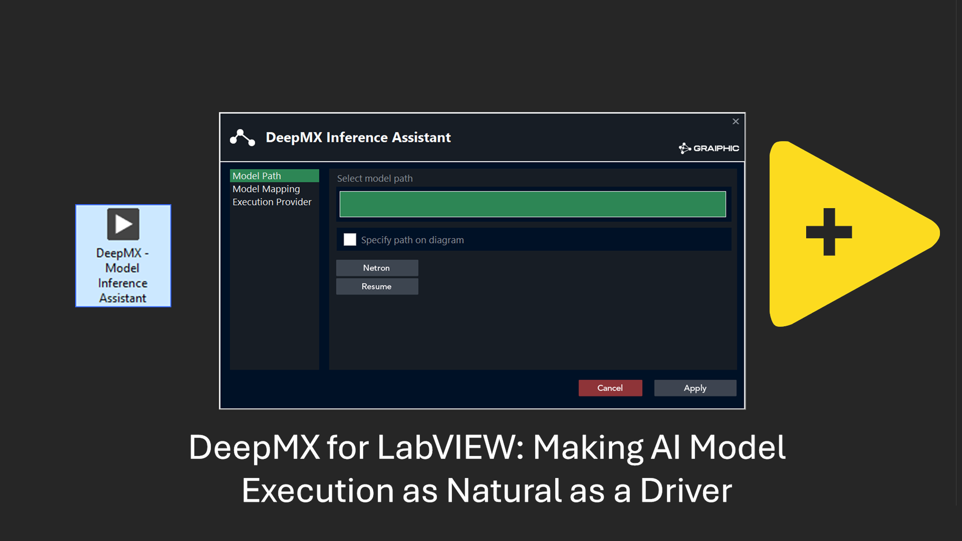
Mini case: Raspberry Pi first
- Scenario: an ONNX model detects an object and drives a GPIO LED using
HWDelay/WaitSyncfor deterministic timing. - Deployment: copy the same .onnx to the Pi; ORT loads compute + hardware EPs; no LabVIEW runtime on the device.
- Value: prototype in hours, then move to Jetson/Zynq without rewriting logic.
Quick FAQ
What if a HW node isn’t supported?
Clear error or software fallback, by policy.
What if the target can’t meet timing contracts?
The runtime reports a contract violation → reschedule or choose an alternate path.
Real‑time capable?
GO HW nodes carry timing/sync attributes; the EP maps to timers/events/DMA to reduce jitter; profiling is built‑in.
Glossary
- AXI/NoC: on‑chip highways connecting SoC blocks.
- DMA: memory transfers offloaded from the CPU.
- EP (Execution Provider): a bridge from ONNX Runtime to a vendor stack.
- Perf/Watt: inferences per watt consumed.
Closing
SoCs are everywhere. Until now, each spoke its own language. With GO HW, a single graph speaks to all, and each target plays to its strengths.
We’ll make it happen: we’ll publish demos, catalog supported hardware (I/O, compute, timing capabilities), and release compatibility matrices that grow version after version.
- Initial, non‑exhaustive list:
- CPUs: x86‑64 (Intel/AMD), ARM64 (Cortex‑A53/A72/A76/Neoverse), selected RISC‑V.
- Edge SoCs: Raspberry Pi 5/4 (BCM2712/2711), Rockchip RK3588/3566, NXP i.MX 8, TI Sitara AM62/64.
- NVIDIA Jetson: Nano, Xavier, Orin.
- FPGAs/SoC‑FPGAs: Xilinx Zynq‑7000/UltraScale+ MPSoC, Versal; Intel Agilex.
- AI accelerators: Intel Movidius, Google Coral Edge TPU, NVDLA/ARM NPUs (via vendor bridges).
- Buses & I/O: GPIO, I²C, SPI, UART, PWM, CAN, MIPI, PCIe, Ethernet TSN (progressive enablement).
Join us: hello@graiphic.io — to test, bring a target, or co‑develop a vendor EP.
Resources
- ONNX — onnx.ai
- ONNX Runtime — onnxruntime.ai
- Graiphic videos — youtube.com/@graiphic
- Articles — graiphic.io/news-insights
Hook
What is a SoC?
A System‑on‑Chip integrates multiple hardware IP blocks:
- CPU (general purpose): Arm, x86 or RISC‑V cores run the OS and control logic.
- GPU: massively parallel compute (graphics, GPGPU, AI kernels).
- NPU/VPU/DSP: dedicated accelerators (neural networks, vision, audio/video, signal processing).
- Memory subsystem: DDR/LPDDR controllers, cache hierarchy, coherency fabrics.
- Interconnect: AMBA/AXI networks or a NoC (network‑on‑chip).
- Peripherals: GPIO, I²C, SPI, UART, PWM, USB, Ethernet, PCIe, MIPI CSI/DSI, CAN.
- Security: secure boot, TEEs, crypto engines.
- Power & clocks: DVFS domains, PLLs, low‑power states.
Why it matters
- Energy efficiency: short data paths → lower dynamic power.
- Low latency: on‑chip hops beat board‑level detours.
- BOM/footprint: fewer chips, smaller boards, lower cost.
- Performance‑per‑watt: the key metric for edge and embedded.
The big families of SoCs (with examples)
- Application Processors (AP): multi‑core CPU + GPU + ISPs + accelerators. Examples: Raspberry Pi 5 (BCM2712), Qualcomm Snapdragon, NXP i.MX 8, Apple M‑series.
- MCU‑class SoCs: lightweight CPUs with on‑chip SRAM/Flash and tight real‑time I/O. Examples: STM32, ESP32.
- AI/Vision SoCs: purpose‑built NPUs/VPUs. Examples: NVIDIA Jetson (Orin/Xavier), Intel Movidius, Google Coral (Edge TPU), ARM NPUs.
- SoC‑FPGAs: CPU + FPGA on one die for cycle‑accurate logic. Examples: Xilinx Zynq/Versal, Intel Agilex SoC.
- Industrial/real‑time SoCs: determinism, functional safety, field buses (CAN, TSN). Examples: TI Sitara AM62/AM64, Renesas families.
Metaphor: think airports. APs are global hubs; MCUs are agile airfields; Jetson/Coral are cargo terminals for AI; SoC‑FPGAs are modular airports where you can draw your own runways.
How software actually runs on a SoC
- Boot stack: Boot ROM → bootloader → kernel (Linux/RTOS) → drivers/services → app.
- Acceleration: schedulers and drivers dispatch work across CPU/GPU/NPU/DSP.
- Physical I/O: drivers expose GPIO/buses/timers; DMA moves buffers off‑CPU.
- Energy control: DVFS and power‑gating scale voltage/frequency per domain.
The plumbing: GPIO, buses, DMA, and clocks
- GPIO: software‑controlled pins; can be debounced, edge‑triggered, or pulled up/down.
- Buses: I²C, SPI, UART, CAN, MIPI, PCIe, Ethernet/TSN.
- DMA: the conveyor belt that moves data with minimal CPU involvement; supports scatter‑gather.
- Clocks & PLLs: the conductor that sets the tempo; DVFS turns it up during crescendos and down between songs to save energy.
A short history: CPU → GPU → NPU → FPGA
- CPU: from early microprocessors to today’s multi‑core designs, CPUs remain the general‑purpose workhorses.
- GPU: born for 3D, generalized with GPGPU; later, Tensor Cores mainstreamed AI math.
- NPU/TPU/VPU: specialized engines for NN ops (conv, matmul, attention) that maximize perf/W on mobile/edge.
- FPGA & SoC‑FPGA: reconfigurable logic with cycle‑level control; ideal for deterministic pipelines and custom interfaces.
Vendors, SoC families — and how they map to ONNX Runtime EPs
Availability varies by OS/toolchain. Here’s a compact map from SoC vendors/families to ONNX Runtime Execution Providers (EPs) you’d typically use:
/////
Key idea: a single ONNX graph can be partitioned across these EPs (compute + hardware) to get the best of each target.
Why GO HW is a step‑change
- GO HW hardware ops:
DMARead,DMAWrite,GPIOSet,HWDelay,WaitSync,ReadTemp, etc., with formal contracts. - Automatic partitioning: AI → compute EPs (CUDA/ROCm/OpenVINO/…); real‑time I/O → GO HW Hardware EP close to the metal.
- One artifact (.onnx) from dev PC to target (Raspberry Pi, Jetson, Zynq, x86 RT…).
- Energy & inference efficiency: right‑place ops, zero‑copy/DMA, event‑driven I/O, quantization/fusion → more inferences per watt.
- Quality & traceability: explicit contracts, vendor API mapping, built‑in tracing and reproducible tests.
Metaphor: GO HW is a conductor with a single score (the ONNX graph). Whatever the venue (the SoC), the orchestra (CPU/GPU/NPU/FPGA) plays the same music with the right sections.
Mini case: Raspberry Pi first
- Scenario: an ONNX model detects an object and drives a GPIO LED using
HWDelay/WaitSyncfor deterministic timing. - Deployment: copy the same .onnx to the Pi; ORT loads compute + hardware EPs; no LabVIEW runtime on the device.
- Value: prototype in hours, then move to Jetson/Zynq without rewriting logic.
Quick FAQ
What if a HW node isn’t supported?
Clear error or software fallback, by policy.
What if the target can’t meet timing contracts?
The runtime reports a contract violation → reschedule or choose an alternate path.
Real‑time capable?
GO HW nodes carry timing/sync attributes; the EP maps to timers/events/DMA to reduce jitter; profiling is built‑in.
Glossary
- AXI/NoC: on‑chip highways connecting SoC blocks.
- DMA: memory transfers offloaded from the CPU.
- EP (Execution Provider): a bridge from ONNX Runtime to a vendor stack.
- Perf/Watt: inferences per watt consumed.
Closing
SoCs are everywhere. Until now, each spoke its own language. With GO HW, a single graph speaks to all, and each target plays to its strengths.
We’ll make it happen: we’ll publish demos, catalog supported hardware (I/O, compute, timing capabilities), and release compatibility matrices that grow version after version.
- Initial, non‑exhaustive list:
- CPUs: x86‑64 (Intel/AMD), ARM64 (Cortex‑A53/A72/A76/Neoverse), selected RISC‑V.
- Edge SoCs: Raspberry Pi 5/4 (BCM2712/2711), Rockchip RK3588/3566, NXP i.MX 8, TI Sitara AM62/64.
- NVIDIA Jetson: Nano, Xavier, Orin.
- FPGAs/SoC‑FPGAs: Xilinx Zynq‑7000/UltraScale+ MPSoC, Versal; Intel Agilex.
- AI accelerators: Intel Movidius, Google Coral Edge TPU, NVDLA/ARM NPUs (via vendor bridges).
- Buses & I/O: GPIO, I²C, SPI, UART, PWM, CAN, MIPI, PCIe, Ethernet TSN (progressive enablement).
Join us: hello@graiphic.io — to test, bring a target, or co‑develop a vendor EP.
Resources
- ONNX — onnx.ai
- ONNX Runtime — onnxruntime.ai
- Graiphic videos — youtube.com/@graiphic
- Articles — graiphic.io/news-insights